
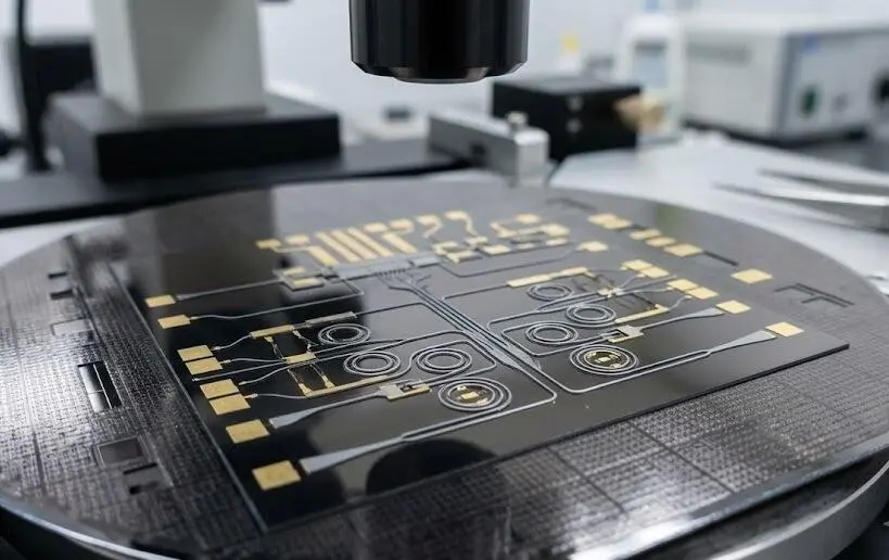
Every video you stream and every question you put to an AI chatbot sets off a flood of data moving between chips, racks and buildings. More and more of that traffic now travels as light instead of electricity. Silicon nanophotonics is the field that makes this possible, using tiny structures etched into ordinary silicon wafers to guide, filter and switch light.
If the term sounds intimidating, don’t worry. This guide explains what silicon nanophotonics is, how it works, where it already earns its keep, and which problems still keep engineers up at night.
Key Takeaways
- The field controls light with silicon structures that are often as small as the light’s own wavelength.
- It reuses the same factories that make computer chips, which is a big reason it can scale.
- Its strongest commercial pull today is moving data inside AI clusters and data centers using less power.
- Silicon is a poor light emitter, so lasers usually come from other materials added to the chip.
- Temperature sensitivity, fabrication variation and fiber coupling remain the biggest hurdles.
- Sensing, LiDAR, optical computing and quantum networks are the next areas to watch.
What Is Silicon Nanophotonics?
Silicon nanophotonics is the study and use of light at the nanometre scale inside silicon structures. The features involved are tiny. A typical light-carrying wire, called a waveguide, is only a few hundred nanometres wide, which is roughly a hundred times thinner than a human hair.
Silicon suits this job because it is transparent at the infrared wavelengths used in fiber-optic communication, around 1.3 and 1.55 micrometres. Light passes through with very little absorption, so a narrow strip of silicon can act like a wire for light.
The “nano” part matters because shrinking structures down to the scale of the wavelength changes how light behaves. It can be trapped, slowed, filtered or boosted in ways that bulky optics simply can’t manage.
How It Differs From Silicon Photonics
The two terms overlap heavily, and many papers use them almost interchangeably. Silicon photonics usually refers to building photonic integrated circuits on silicon, mainly for communication. Silicon nanophotonics puts the spotlight on nanoscale effects such as resonances, tight confinement and strong light-matter interaction.
A simple way to remember it: one is about the circuit, the other is about the physics that makes the circuit small and powerful.
A Short History of Silicon Nanophotonics
Putting optics on silicon, the idea behind silicon photonics, isn’t new. Researchers noticed long ago that the material used for transistors could also guide infrared light, and that an enormous manufacturing base already existed.
The first big commercial wins came from optical transceivers, the modules that turn electrical signals into light and back again for telecom and data center links. Those products proved that photonic chips could be built in volume, and they grew a supply chain of foundries, packaging houses and test equipment.
Nanoscale design followed as fabrication improved. Finer lithography let engineers etch features small enough to build compact resonators and photonic crystals, which moved silicon nanophotonics from simple waveguides toward dense circuits and sensors.
How Silicon Nanophotonics Works
Why Silicon Traps Light So Well
Light stays inside a material when that material has a higher refractive index than its surroundings. Silicon’s refractive index is about 3.5, while silicon dioxide, the glass it usually sits on, is around 1.45. That large gap works like a very strong fence for light.
Because of it, waveguides can bend sharply and circuits can be packed tightly. Most devices are built on silicon-on-insulator wafers, which have a thin silicon layer on top of an oxide layer on top of a regular silicon wafer.
The Core Building Blocks
Most nanophotonic devices are assembled from a small toolkit of parts:
- Waveguides carry light across the chip.
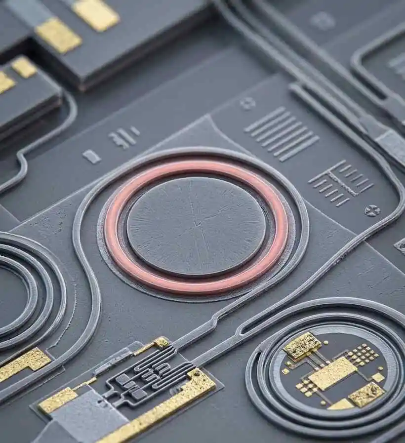
- Microring resonators filter or switch specific wavelengths, and can also act as compact modulators.
- Modulators write data onto light. Silicon lacks a strong direct electro-optic effect, so most designs change the density of charge carriers to alter the refractive index.
- Photodetectors turn light back into electric current. Germanium is grown on silicon for this, since silicon itself is nearly blind at telecom wavelengths.
- Couplers move light between optical fiber and the chip.
- Lasers supply the light. These typically come from other semiconductor materials, which we’ll return to shortly.
Nanostructures That Squeeze Light Further
Beyond basic circuits, researchers pattern silicon with holes and tiny blocks to push light harder. A photonic crystal cavity, for example, uses a repeating pattern of nanoscale holes to hold light in a very small space for a surprisingly long time. That boosts how strongly light interacts with anything placed inside.
Small silicon particles can also support Mie resonances, which concentrate light and strengthen nonlinear effects. Experiments in recent years show that silicon nano-resonators can respond to light far more strongly than bulk silicon, and that this response can change within picoseconds. That opens doors for ultrafast optical switching and new imaging methods.
Metasurfaces and Flat Optics
Silicon nanophotonics is not only about circuits. Metasurfaces are flat surfaces covered with arrays of tiny nanostructures that change the phase, strength and polarization of light passing through or bouncing off them. Because each element can be tuned, one thin layer can do the work of a bulky lens.
Silicon performs well for this at near-infrared wavelengths, but it absorbs visible light, so visible-light designs usually rely on other materials. Ultra-thin lenses, beam steering and compact imaging are active research areas.
Choosing a Platform: Silicon, Silicon Nitride or Lithium Niobate
No single material does everything well, so a modern silicon nanophotonics platform often mixes several. Here is how the three most common options compare in general terms.
| Platform | Strengths | Trade-offs |
| Silicon-on-insulator | Tight light confinement, compact circuits, mature manufacturing, good germanium detectors | Weak light emission, no strong linear electro-optic effect, two-photon absorption at high power |
| Silicon nitride | Low waveguide loss, handles higher optical power, less temperature drift | Lower index contrast means larger devices, and no built-in modulation or detection |
| Thin-film lithium niobate | Strong electro-optic effect for fast, efficient modulators | Harder to integrate at scale and less aligned with standard chip lines |
How the Chips Are Made
Silicon nanophotonics chips follow the same core steps as electronics: lithography draws the pattern, etching carves it, and deposition adds new layers. Nanometre precision matters because tiny size changes shift how light behaves.
Foundries that offer photonics usually provide a process design kit, a rulebook plus a library of tested components, so designers don’t start from scratch. Shared multi-project wafer runs let several teams split one wafer, which lowers prototyping costs for universities and startups building photonic integrated circuits.
Key Terms in Plain English
- Refractive index: a measure of how much a material slows light down. Higher values trap light more tightly.
- Bandgap: the energy gap that decides whether a material absorbs or emits a given color of light.
- Quality factor (Q): how long a resonator holds on to light. A higher Q means sharper, more sensitive devices.
- Wavelength division multiplexing: sending several colors of light, each carrying its own data, down the same waveguide.
- Co-packaged optics: placing the optical engine in the same package as a switch or processor to shorten electrical paths.
Why Silicon Nanophotonics Matters Right Now
Copper wires are running into physical limits. As data rates climb, electrical signals lose more energy to resistance and heat, and they can’t travel far at high speed without help. Moving data between chips now takes a large share of a system’s energy budget. That makes lower-energy data movement a sustainability story, not just a speed story.
Optical interconnects play by different rules. Waveguides lose very little signal over chip-scale distances, and many wavelengths can share one waveguide through wavelength division multiplexing. The energy cost also stays fairly steady as a link gets longer, which electrical wires can’t match.
There’s a business reason too. Photonic integrated circuits can be made in existing semiconductor foundries on 300 mm wafers. That means mass-production economics, rather than lab-only craftsmanship, apply to light-based hardware.
5 Powerful Uses of Silicon Nanophotonics
1. Data Centers and AI Clusters
This is where the money is flowing today. Training large AI models needs thousands of processors to swap data constantly, and copper links are turning into a power and bandwidth bottleneck.
Optical interconnects built on silicon chips already link data center switches. The next step is co-packaged optics, which places the optical engine right beside the switch or processor. Nvidia has announced co-packaged optical switches for 2026, and the specialist company Ayar Labs raised $500 million in March 2026 to scale up production. Analysts expect pluggable, near-package and co-packaged optics to coexist for some years.
2. Optical Networks Inside Processors
As core counts rise, electrical networks-on-chip struggle to keep up. Optical networks-on-chip route data between cores using light, offering high bandwidth through wavelength multiplexing and little change in energy as distance grows.
The catch is static power. Lasers and ring tuning draw power even when no data is moving. A recent survey of the field names this as a major issue, along with security questions when third-party hardware blocks share the same optical network.
3. Optical Computing and AI Accelerators
Some of the most interesting nanophotonic devices don’t just move data, they compute with it. Light passing through a mesh of interferometers can perform matrix multiplication, the core operation in neural networks, at very high speed.
Startups such as Lightmatter and Lightelligence are pursuing this path. Still, precision, converting between electrical and optical signals, and programming remain open problems. Expect photonics to complement electronic processors first, not replace them.
4. Sensing, Biosensing and LiDAR
A microring resonator is extremely sensitive to what touches its surface. When molecules bind, the local refractive index shifts and so does the resonant wavelength. That lets chip-sized sensors detect biomolecules without fluorescent labels, and the same idea supports gas and environmental sensing.
This platform also supports solid-state LiDAR, where optical phased arrays steer laser beams with no moving parts. Automotive companies have explored it for years as a way to cut cost and size.
5. Quantum Technologies
Photons are excellent carriers of quantum information, and silicon chips can route them with precision. Researchers are building quantum photonic circuits on silicon to generate and manipulate photon states.
A newer line of work embeds single rare-earth atoms, such as erbium, into silicon resonators to create quantum memories. Erbium emits near 1.5 micrometres, right in the telecom band, which makes it a natural fit for future quantum networks. It’s still lab research, but it shows how far the field reaches.
Closely related is work on coupled-cavity networks, where light hops between neighboring nanoscale resonators. Because each cavity concentrates light so strongly, very little optical power can be enough to change how the network responds, which is why silicon nanophotonics researchers study these structures for ultra-low-power optical switching and for linking quantum emitters.
Challenges Silicon Nanophotonics Still Has to Solve
The technology is promising, but it isn’t magic. These are the hurdles that matter most.
Silicon Can’t Make Light Efficiently
Silicon has an indirect bandgap, so electrons rarely release their energy as light. Engineers work around this by bonding III-V semiconductor lasers to silicon, growing germanium or quantum-dot lasers on it, or feeding in light from external lasers. Each route adds cost or complexity.
Heat and Tiny Fabrication Errors
Many nanophotonic devices, resonators especially, shift wavelength as the temperature changes, and even a nanometre-scale difference in width during manufacturing moves it off target. Heaters correct the drift, but they use power and add control circuitry.
Getting Light In and Out
Aligning an optical fiber to a chip with sub-micrometre accuracy is difficult. Coupling loss, packaging cost and test yield all become serious when optical interconnects sit inside the same package as expensive processors, because a faulty part is hard to rework.
Polarization and Thermal Crosstalk
Waveguides respond differently to different polarizations of light, so designers must control polarization or operate with a single one. On a dense chip, heat from one device can also drift its neighbors, a problem known as thermal crosstalk.
Nonlinear Losses at High Power
At high optical intensity, silicon absorbs light through two-photon absorption, and the free carriers this creates absorb even more. That caps the power a waveguide can carry, so designers turn to materials such as silicon nitride when high power is needed.
What Comes Next for Silicon Nanophotonics
Expect heterogeneous integration to define the next decade. Instead of forcing silicon to do everything, designers are building photonic integrated circuits that combine it with III-V lasers, germanium detectors, silicon nitride waveguides and thin-film lithium niobate modulators.
Design tools are changing too. With inverse design, software searches for the structure that best meets a performance goal, often producing odd, non-intuitive shapes that beat hand-drawn ones. Many nanophotonic devices could be designed this way, as long as the result can still be manufactured at nanometre precision.
In the near term, the clearest growth path is AI infrastructure, where power budgets are tight. Further out, optical I/O chiplets, neuromorphic photonics and quantum networking could widen the field. Timelines in this industry slip often, so treat bold forecasts with healthy skepticism.
Faqs
What is silicon nanophotonics used for?
Silicon nanophotonics is used mainly for high-speed data transfer in data centers and AI clusters. It also powers chip-scale sensors, LiDAR, early optical computing hardware and experimental quantum devices.
What is the difference between silicon photonics and silicon nanophotonics?
The first focuses on building photonic circuits on silicon, mostly for communication. The second emphasizes nanoscale structures and the strong light-matter effects they produce. In practice the fields overlap, and the terms often appear together.
Why is silicon used for nanophotonics?
Silicon is transparent at telecom wavelengths, has a high refractive index that keeps light tightly confined, and can be processed in existing CMOS factories. Those traits make the technology both compact and affordable to produce.
Can silicon emit light?
Not efficiently. Its indirect bandgap makes light emission weak, which is the central reason silicon nanophotonics relies on lasers made from III-V materials or other external sources.
What are the biggest challenges of silicon nanophotonics?
Integrating efficient lasers, managing heat and fabrication variation, cutting static power, and coupling light between fiber and chip. Packaging yield also matters more as optics move closer to processors.
Bottom Line
Silicon nanophotonics takes the manufacturing muscle of the chip industry and uses it to steer light instead of electrons. Its biggest payoff today is faster, cooler data movement for AI, with sensing, optical computing and quantum networking close behind.
The obstacles are real, especially around lasers, heat and packaging, yet steady progress keeps shrinking them. If you follow one trend in computing hardware over the next few years, silicon nanophotonics deserves a spot on the list.